![[회전]Research_banner.png](https://static.wixstatic.com/media/977c5b_0f28290b44354228a06b67b4f31cea20~mv2.png/v1/fill/w_980,h_134,al_c,q_85,usm_0.66_1.00_0.01,enc_avif,quality_auto/977c5b_0f28290b44354228a06b67b4f31cea20~mv2.png)
Research
Research Area
Electron Microscopy (TEM/SEM)
Electron microscopy, particularly transmission electron microscopy (TEM), is one of the most powerful and versatile techniques for probing the physicochemical and structural properties of materials. By exploiting the extremely short wavelength of high-energy electron beams, TEM enables direct exploration of materials at the nano- and atomic scales.
Our laboratory actively utilizes and advances a wide range of scanning and transmission electron microscopy (SEM/TEM) techniques to investigate reaction mechanisms in batteries and ferroelectric materials, providing atomic- and nanoscale insights into their structure–property relationships.


01. In-situ TEM/SEM
In-situ TEM and SEM, which allow real-time observation of materials, provide unique insights into reaction dynamics with high temporal resolution—essentially capturing “movies” rather than static images. These techniques enable us to directly observe how materials respond to external stimuli such as electrical current, voltage, heat, or mechanical stress.
We can even create liquid environments within the high-vacuum TEM column to study reactions under realistic operating conditions, a method known as operando TEM. Using state-of-the-art in-situ and operando TEM/SEM, our laboratory investigates the atomic- and nanoscale behavior of materials in batteries and ferroelectrics under various stimuli.
Our goal is to lead the development of in-situ and operando electron microscopy techniques while exploring previously uncharted atomic and nanoscale phenomena, contributing both to fundamental knowledge and technological innovation.

[Operando TEM liquid cell design
for lithium metal battery studies]

[Chemical mapping of SEI on Li,
deposited in the operando TEM experiment]
[Operando liquid-phase TEM experiments for lithium metal battery studies:
(left) Li dendritic and (right) Li nanogranular growth behaviors]
S. –Y. Lee et al., Energy & Environ. Sci. 13, 1832 (2020) (Link)
S. –Y. Lee et al., Nano Energy 102, 107641 (2022) (Link)
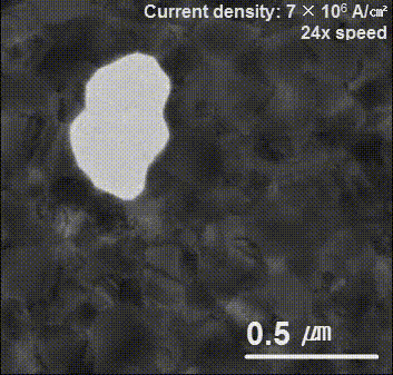
[In-situ I-V TEM: Cu electromigration path]

[Cu crystal orientation map]
Y. –H. Oh, S. –Y. Lee* et al., Ultramicroscopy 181, 160 (2017) (Link)

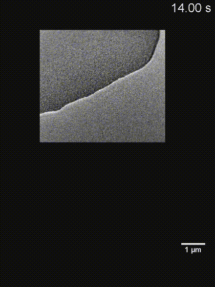
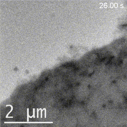
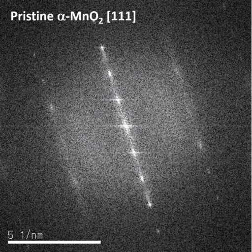
[In-situ I-V TEM: Li-ion insertion reaction of MnO2 nanowire electrode for Li-ion batteries]
[In-situ I-V TEM: HRTEM-FFT video]

[In-situ I-V TEM: EELS]
02. Cryo-TEM
Cryo-TEM is a technique in which specimens are cooled to extremely low temperatures near that of liquid nitrogen, allowing them to be observed in their original state while minimizing damage from the electron beam. This approach is particularly valuable for materials that are highly sensitive to electron irradiation.
In our laboratory, we utilize Cryo-TEM to directly visualize lithium metal, which is especially vulnerable to beam damage, in its intact form. This enables us to analyze the morphology and chemistry of lithium that grows or detaches during battery operation, providing precise insights into the reaction mechanisms and performance degradation of lithium metal batteries.

[Cryo-TEM study for elucidating LiNO3 additive effect in lithium metal batteries]
S. –Y. Lee group, J. Energy Chem. 114, 485 (2025) (Link)
03. Machine learning
Despite the power of TEM, data quality can still be limited due to the specific nature of the specimens and measurement conditions, leaving many fundamental aspects of materials’ behavior unexplored. Moreover, certain features remain beyond the ability of human observation to distinguish.
Our laboratory leverages machine learning techniques to enhance both the quality and interpretability of TEM data, including EELS, imaging, and 4D-STEM datasets. By maximizing the potential of TEM through these advanced computational approaches, we aim to uncover previously inaccessible atomic-scale reaction behaviors in a wide range of materials.

04. 4D-STEM (4D-STEM-ASTAR)
4D-STEM (4D-STEM-ASTAR) is a cutting-edge technique in which a 2D area is scanned pixel by pixel, recording a 2D electron diffraction pattern at each pixel. This approach enables detailed analysis of subtle, nanoscale variations in crystal structure across a material.
In our laboratory, we apply 4D-STEM-ASTAR to perform in-depth structural analysis of battery electrode materials and ferroelectric materials. Beyond this, we are developing methods to quantify single crystallinity in single-crystal cathode particles using this technique, advancing the precision and capability of crystallographic analysis at the nanoscale.

[Development of a quantitative method to calculate single crystallinity of lithium-ion battery cathodes using 4D-STEM-ASTAR]
S. –Y. Lee group, J. Mater. Chem. A 12, 9863 (2024) (Link)
05. Atomic structure
Scanning electron microscopy (SEM) allows us to explore materials at the micron to tens-of-nanometers scale, while transmission electron microscopy (TEM) extends our view to the nanoscale and even down to individual atoms. By directly observing atoms with TEM, we gain fundamental insights into the behavior of a wide range of materials.
In our laboratory, we combine SEM and TEM to perform multi-scale characterization, enabling a comprehensive understanding of materials across length scales. In addition, we integrate other complementary techniques, including X-ray photoelectron spectroscopy (XPS), X-ray diffraction (XRD), electrical/electrochemical measurements, etc., to precisely elucidate the mechanisms that govern material performance.
[SEM image of Li-ion battery cathode material]
[Orientation mapping at nanoscale]
[Atomic resolution STEM image]
